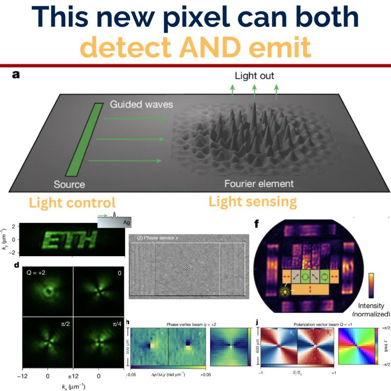
Every pixel since the first CCD does one thing: detect OR emit light. ETH Zurich just ended this constraint. In a 10µm element pixel can detect and emit: The Norris group at ETH Zurich uses surface plasmon polariton waves (coherent electromagnetic waves propagating along metallic surfaces) as intermediaries. When these plasmons hit precisely designed wavy microstructures, they scatter into arbitrary optical wavefronts. Run it in reverse, and incoming light couples back into the plasmons, fully characterizing the field. The design requires no electromagnetic simulation. The inverse Fourier transform of the wavefront you want gives you the surface profile to fabricate, which takes about one day from concept to working device. As a result full control over amplitude, phase and polarization, in both sensing and generation is possible. With this method a >40% power efficiency across 500 to 700nm is possible.