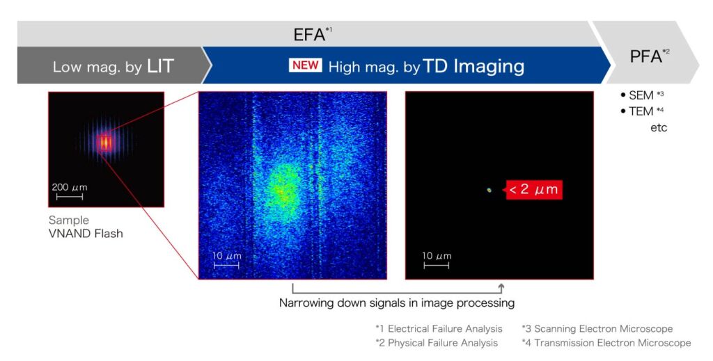
Hamamatsu Photonics introduces ThermoDynamic Imaging (TDI) for their new Phemos series. TD Imaging is suitable for identifying defects in semiconductors with complex structures, such as logic semiconductors. It is available to pinpoint defects in semiconductors that contain metal parts internally. The patended laser scan technollogy improves signal-to-noise ratio (SNR) by 38 times, delivering high precision and reliability in thermal imaging. 670 or 1,300nm light source enhances SNR for Cu and Al. Flexible scan speed, size, and integrations, with data acquisition in 90 seconds for higher SNR than LIT.