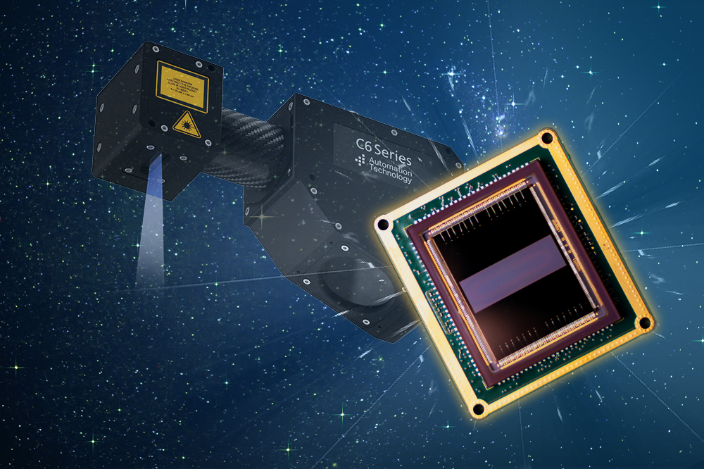
In the combination of resolution and speed, the 3D sensors of the C6-3070 series by AT Automation Technology impress with the new WARP technology (Widely Advanced Rapid Profiling). The reason for the fast 3D scans is the on-chip processing of the 3D sensor chip developed in-house. This detects the laser line and compresses it without loss using intelligent algorithms. This enables the sensor to achieve a 3D profile pixel rate of, for example, 128MP at an ROI of 200 lines with a profile speed of 42 kHz. To be able to achieve the highest possible profile rates, ROIs are first defined within the sensor. In addition, region tracking is available to maximize reliability. This has the advantage that the ROI is also optimally positioned around the laser line for components that move during the measurement process.